By Vishal Goel, | January 21, 2017
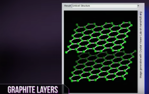
Graphene is only 0.3 nanometers thick and consists of a single layer of carbon atoms assembled in a kind of honeycomb pattern. (YouTube)
For the first time, graphene, the world's second toughest material, has been used to develop functional organic light-emitting diode (OLED) electrodes. An OLED produces brighter light and uses less energy than existing LCD and LED technologies.
Thanks to a breakthrough by German researchers, OLED electrodes can now be integrated into touch displays to pave the way for a variety of smart material applications.
Like Us on Facebook
Scientists from the Fraunhofer Institute for Organic Electronics and Electron Beam and Plasma Technology (FEP) partnered with industry and researchers to create the electrodes with an area of 2×1 square centimetres under an EU-funded project named "Gladiator" (Graphene Layers: Production, Characterization and Integration) launched in November 2013. As FEP's project leader Dr. Beatrice Beyer said that this is a real breakthrough in the field of research and integration of extremely demanding materials.
About Graphene
Graphene is considered a miracle material because the advantages of this carbon compound are impressive. It:
- is light
- is transparent
- is extremely hard
- has more tensile strength than steel.
- is flexible and extremely conductive for heat or electricity.
Graphene is only 0.3 nanometers thick and consists of a single layer of carbon atoms assembled in a kind of honeycomb pattern.
How are OLED electrodes made?
The production of the electrodes takes place in a vacuum. A wafer plate of high-purity copper is heated to about 800 degrees in a steel chamber. Then a mixture of methane and hydrogen is supplied which initiates a chemical reaction. The methane dissolves in the copper and forms carbon atoms, which spread on the surface. This process takes only a few minutes. After a cooling phase, a carrier polymer is placed on the graphene, and the copper plate is etched away.
Currently, the team is working on minimizing the impurities and defects which occur during the transfer of the wafer-thin graphene to another carrier material.


-
Use of Coronavirus Pandemic Drones Raises Privacy Concerns: Drones Spread Fear, Local Officials Say

-
Coronavirus Hampers The Delivery Of Lockheed Martin F-35 Stealth Fighters For 2020

-
Instagram Speeds Up Plans to Add Account Memorialization Feature Due to COVID-19 Deaths

-
NASA: Perseverance Plans to Bring 'Mars Rock' to Earth in 2031

-
600 Dead And 3,000 In The Hospital as Iranians Believed Drinking High-Concentrations of Alcohol Can Cure The Coronavirus

-
600 Dead And 3,000 In The Hospital as Iranians Believed Drinking High-Concentrations of Alcohol Can Cure The Coronavirus
-
COVID-19: Doctors, Nurses Use Virtual Reality to Learn New Skills in Treating Coronavirus Patients
